US chip manufacturer SkyWater Technology and Google Public Sector are expanding an open source platform to design chips that can be made in SkyWater’s Minnesota facility.
SkyWater said the US Department of Defence is funding US$15 million (S$20 million) for the development of the platform.
“One of the reasons the US government is investing in this initiative is because they can then take the output of a lot of this development,” SkyWater CEO Thomas Sonderman said.
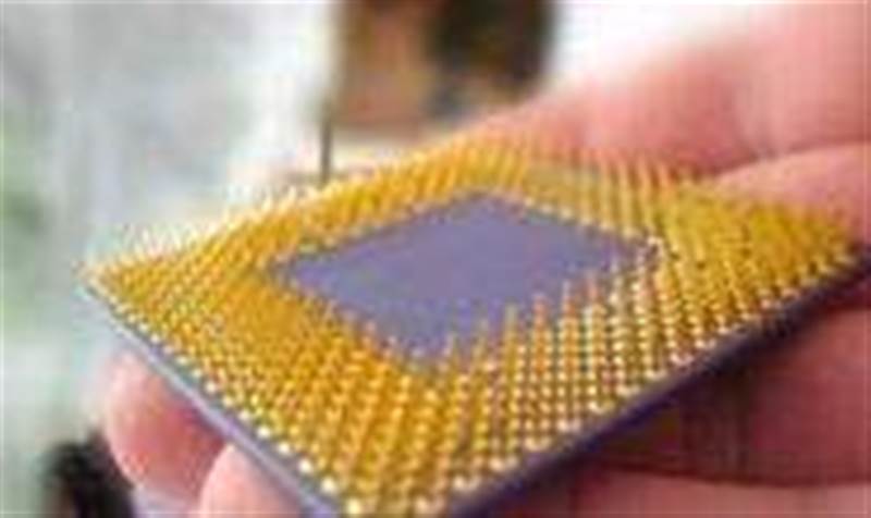
Chip design and manufacturing is a very expensive process. Not only is chip design software, called electronic design automation, or EDA, expensive to license, but making the first test chips in fabrication facilities can cost tens of thousands of dollars.
“We’re hoping that the collaboration is going to address what are really historical limitations of chip design and production, both for national defence as well as commercial markets, because researchers get improved accessibility and developers get to go through that exploration faster and candidly at lower costs,” said Will Grannis, CEO of Google Public Sector.
Google Public Sector, a for-profit subsidiary of Google, was launched in June to better work with the government and education institutions, said Grannis.
The chip design platform will be powered by Google and live on Google’s cloud, he said.
This is the second chip design platform project that Google and SkyWater have worked on.
The first was a platform for chips that could be manufactured on SkyWater’s 130-nanometer process. The latest one is for the production of chips on SkyWater’s 90-nanometer process.
Sonderman said the platform is for analogue-digital mixed-signal chips often used in things like smart home products.
Such chips can take advantage of larger transistors, such as 90 nanometer, for cheaper production, he said.